Figure 1. Hybrid crystal footprint
Crystal Oscillator General PCB Layout Guidelines
We will outline the general crystal oscillator PCB layout guidelines. All of these guidelines have a good intention, however not all of them are equally important in every case. That’s why we will discuss two design cases.
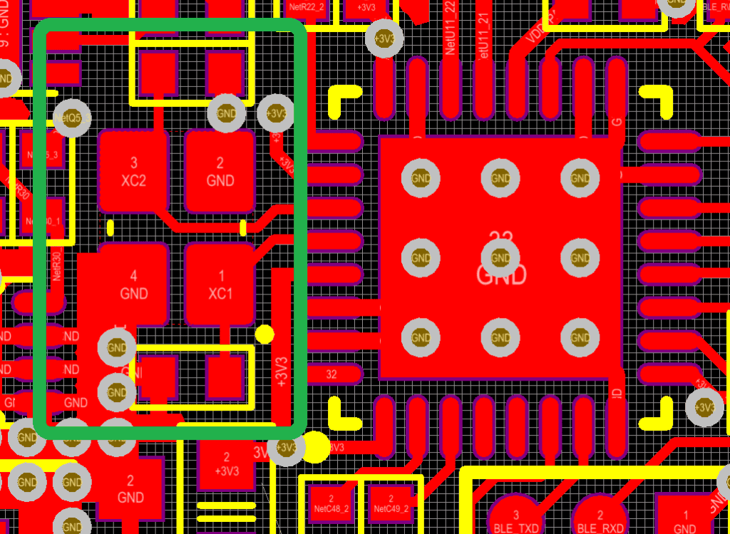
- Place all oscillator components as close as possible to the oscillator IC pins.
- Keep the load capacitors and series resistor as close as possible to the crystal.
- Keep high frequency (and fast rise time) components as far away as possible to the oscillator to avoid capacitive coupling.
- Keep the oscillator traces as short and straight as possible. This will reduce the chance of coupling.
- Keep the area under the crystal well-grounded.
- The ground connection for the load capacitors should be short and avoid the return currents from the fast communication interfaces.
- In case you use a single layer PCB, place the GND guard ring around all oscillator components and oscillator GND pin.
- Place oscillator as far as possible from potential heat sources (power components, RF transmitters…)
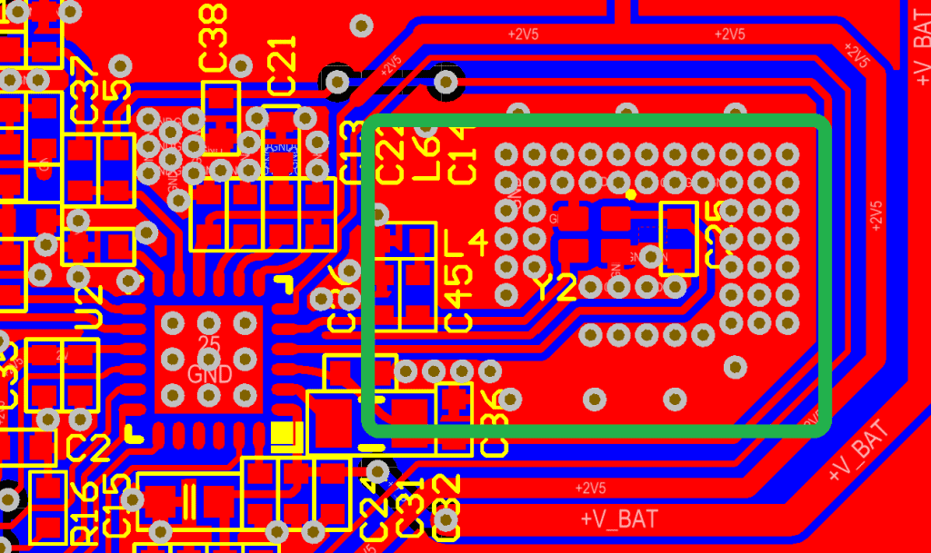
Digital System Oscillator Layout
In the majority of digital systems, the frequency accuracy and stability requirements are in the range of 10s of ppm. For this purpose, the nice simple and clean crystal, load capacitors and resistor placement will do the job perfectly fine. Simply lay them out as close as possible to the oscillator IC pins (same PCB side as the IC, e.g. top side), stitch the GND vias, and pour the bottom side (or the first internal layer) in a nice solid GND.
In most of the cases, there is no need for any GND isolations. If you are on a two-layer PCB, route the analog sensitive traces away from this region, as well as the digital aggressors (follow the above guidelines 1 to 6). If you are on a multi-layer PCB, simply ensure you have a clean GND plane between the oscillator and other traces.